Engineering 44 Fall 2017

Tuesday, October 31, 2017

10/31/17 Second Order Series RLC Circuit Step Response (Under Damped & Critically Damped)

Second Order Series RLC Circuit Step Response


Overview 

           Model and test series RLC second order circuits.
           Part 1 - analyze step response of given circuit.
           Part 2 - Redesign circuit so its critically damped without affecting natural frequency. 

PART1 UNDER Damped Series RLC Circuit:


Pre-Lab 

          a) Write out differential equation relating V(out) and V(in).

          b) Estimate natural frequency, damping ratio, DC gain, period of oscillation 

a) 


b) Natural frequency 


Damping Ratio 


DC gain 

at T = INFINITY (STEADY STATE)

Period of oscillation 


LAB 

Construct circuit using 2 volt step input and a low frequency so that the circuit can reach a steady state before each pulse. 

Results


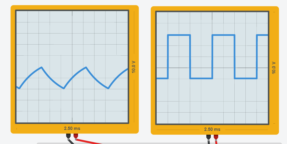
 We can see from the V(out) Oscilloscope on the top right of the figure below  that the RLC circuit is UNDERDAMPED as predicted in the prelab. The oscilloscope on the left is V(in) of the 2v square wave, and the right shows the oscillations of V(out).
Underdamped 2nd order RLC circuit using TINKERCAD


Underdamped RLC series circuit using EveryCircuit 


ANIMATION of Underdamped RLC circuit using EVERYCIRCUIT.

PART 2 CRITICALLY Damped Series RLC Circuit:

Prelab 

             Redesign circuit so its critically damped without affecting natural frequency. 

Changing the resistor from 1.1 to 200 should make circuit critically damped.

LAB 

Modify Circuit from Part 1 to create critically damped circuit without affecting natural frequency. 


Results 

RLC circuit is critically damped with resistor changed to 200 ohm's. Since L, and C are unchanged, natural frequency remains the same as in part 1.
The image below shows the circuit on a breadboard similar to Part 1, where the only change is the resistor from 1.1 to 200 ohms which gives a reading of critically damped as expected from prelab of Part 2 where there is no oscillations in V(out).  


Critically Damped RLC circuit using TinkerCad App


We can see with the figure below, that V(in) is represented in orange and V(out) is represented in green, which shows no oscillations which is critically damped compared to Part 1 that was underdamped with oscillations.
Critically damped RLC series circuit using EveryCircuit.


Animation of Critically Damped RLC circuit on EveryCircuit

Tuesday, October 17, 2017

10/17/17 Active RC Circuit Step Response

Active RC Circuit Step Response

Date: 10/17/17

Overview

Gain an understanding of passive versus active first order circuits. Passive circuits are useful in signal conditioning but arn't good at receiving additional loads which would require redesign of the circuit anytime a different load is applied to the circuit.

Active circuits are somewhat immune to different loads because the power supply comes from external sources. 


Lab Procedures 

1) Construct circuit from circuit diagram above, using resistors of 470  and a capacitor at 1ยตF.

2) Using a function generator, apply 4 volt peak-to-peak square water input with perioes = 10 ms (frequency = 100Hz)


3) Increase frequency to 300Hz, 500Hz, 1,000Hz, and 2,000Hz and comment on behavior. 

Results

(100Hz)

Active RC circuit using op-Amp741 with  square wave Voltage input of 100Hz.


The figure below illustrates the capacitor voltage charge vs discharge at 100Hz, resulting in a saw tooth like wave. 

http://www.electronics-tutorials.ws/rc/rc_3.html


adf

(300Hz)

Oscilloscope showing square wave Voltage input of 300Hz


(500Hz)


Oscilloscope showing square wave Voltage input of 500Hz

(1,000Hz)

Add caption


Oscilloscope showing square wave Voltage input of 1,000Hz

(2,000Hz)


Oscilloscope showing square wave Voltage input of 2,000Hz


Animation of Ramp of Active RC Circuit Step Response via GIPHY

Troubleshooting 

We didn't take photos of our lab because we knew we did it wrong. Our readings on the Oscilloscope where we had one channel for Voltage(in) and one channel for Voltage(out) resulted in the square wave for Voltage(in) which is correct but our Voltage(out) was noisy, with no pattern. We tried troubleshooting over two lab periods where a lab partner constructed his own op-Amp circuit where we got the same incorrect reading for Voltage out. Below was an attempt where voltage out matched Voltage in which is incorrect. I was able to figure out why all of our op-Amps were not giving us the desired outcome when using independent power sources because Vcc(+) and Vcc(-) were not connected correctly.  Turns out that we needed two power sources, one for  Vcc(+) and one for Vcc(-). 

The second figure below was using a resistance load between Voltage (out) and ground giving what we first thought was closer to Ramp but we were incorrect as well. 


With incorrect Vcc(+) and Vcc(-), V(out) reading is the same as V(in) which is incorrect, should be Ramp wave.


Adding a resistance load between V(out) and ground, resulted in an usual wave pattern different than V(in), but error resulted because op-Amp was not connected correctly at Vcc(+) and Vcc(-).  

Tuesday, October 10, 2017

10/10/17 Non - Inverting Amplifier

Non - Inverting Amplifier


Date: 10/10/17

Overview 

            Gain an understanding of simple single operational amplifier-based circuit that are commonly used in circuits used to implement mathematical operations such as voltage gain within a circuit. 

In this lab, we will gain an understanding of a non-inverting op-Amp (op-Amp27) circuit diagram and how to complete the circuit using a 8-pin op-Amp and see the relationship between Voltage(in) and Voltage(out).


Pre-Lab

          a) Find gain ( Vout / Vin ) in the circuit.


(independent power sources)
(using Analog Discovery)

             b)  Why is the circuit called a non-inverting voltage amplifier?
               A inverting op-Amp provides an inverted polarity gain from voltage input in respects to voltage output, where as a non-inverting op-Amp provides a positive voltage gain.

Lab Procedure 

            c)   Apply +5 volts to Vcc(+) and -5 volts to Vcc(-)
            d)  For Voltage input,  go from –3 volts to +3 volts in increments of .5 volts. Record results.
            e) find slope

Results (using both analog discovery and independent power sources)


Non-inverting op-Amp27 using Analog Discovery

Non-Inverting opAmp27 using independent power sources


Data collected for V(in) and V(out) 

(analog discovery)

(data for analog discovery circuit)


(independent power sources)


(independent power sources)


Plot of data

(analog discovery)

(non inverting op-Amp27 using Analog Discovery)

(non inverting op-Amp27 using Analog Discovery)
Slope (gain) = 2.5, which equals the same gain from prelab for analog discovery

(independent power sources)

(independent power sources)

(independent Power Sources)
Slope (gain) = 3, which equals the same gain from prelab for independent power sources


Conclusion 

        At first, like our inverting op-Amp, we weren't able to figure out how to make the circuit using independent power sources so our group, along with other groups ended up using Analog Discovery. We got the help from Kyle to make the analog discovery circuit. I then went home and tried multiple using independent power sources because previous labs and future labs didn't work after figuring out how to do the Inverting op-Amp, I re-did the non-inverting op-Amp. 
Our calculated voltage out for both circuits matched 100% with the actual voltage out resulting in 0% error. I used TinkerCad App to try troubleshoot the independent power sources because I don't have a personal analog discovery tool to retry at home. 


Below is both TinkerCad App and EveryCircuit. 


(non-inverting op-Amp741 using TinkerCad App for independent power  sources)
jkh
(non-inverting op-Amp using EveryCircuit)


Thursday, October 5, 2017

10/5/17Summing Amplifier

Summing Amplifier 

Date : 10/5/2017

Overview

        Summing two voltage inputs into a op-Amp commonly used in circuits to implement mathematical operations.

The output voltage is an inverted and scaled version of the sum of the input voltages Va, and Vb. If R1 = R2, the input voltages are not individually scaled and the output voltage.
Note: R3 = R1, the output voltage is simply the sum of the two input voltages.
given circuit diagram of summing op-Amp


Pre-lab

Design an inverting summing circuit which performs an addition of two voltage inputs. Note, circuit has a virtual ground.

Lab Procedure

For 5 volts for Vcc(+) and Vcc(-)
Set Vb to 1 volt.
Set Va to -4,-2,-1,0,1,2,3, and 5 volts. Record results


Results 

Summing op-Amp741 circuit


Data 


Graph of Voltage (out) versus Voltage (a + b)

Comments

Our results for our summing op-Amp regarding the calculated and actual were identical when using the op-Amp 741. I went ahead and when beyond the voltage input for Va to get values of positive and negative saturation. As seen, when values are within non saturation, and when R3 = R1, the output voltage is simply the sum of the two input voltages. 

Below is verification the circuit using both TinkerCad and EveryCircuit to get a visual representation of the summing op-Amp. 
 Our calculated and actual values for Op-Amp741  matches the calculated value in TinkerCad App.


Summing op-Amp using EveryCircuit App, our calculated, actual and virtual match agree for Vout when Va = 1, Vb= 1, resulting in Vout = -2


Tuesday, October 3, 2017

10/3/17 Inverting op Amp

INVERTING VOLTAGE AMPLIFIER

Date: 10/3/17

Overview 

            Gain an understanding of simple single operational amplifier-based circuit that are commonly used in circuits used to implement mathematical operations such as voltage gain within a circuit. 

In this lab, we will gain an understanding of a inverting op-Amp circuit diagram and how to complete the circuit using a 8-pin op-Amp and see the relationship between Voltage(in) and Voltage(out).

Voltage (out)  is an inverted (due to the sign change) and amplified or scaled (due to the multiplicative factor R2 / R1 version of the input voltage. The scaling factor R2/R1 is called the gain of the amplifier.


The pins for a OP27 op-Amp, or 741 op-Amp, (both single op-Amps),  we can see where pins in a circuit are placed on an 8 pin op-Amp. Pins 1,5,8 don't have any connections in this lab. Pin 5 doesn't connect to any part of a circuit, it's simply there to stabilize the op-Amp when placed in a circuit board. 


Lab Procedure 


Create inverting op-Amp.
Test input voltages from -3V to +4V by step sizes of .5V and record both input and output voltages.
Calculate  circuit gain.


Prelab 

       Calculate Voltage (out) from any by inserting any Voltage. I choose 2 Volts, resistors 22k  for R1, and 44k for R2.


Results 


Op-Amp 27 Circuit


Data and graph of Voltage (in) and Voltage (out) :


Comments


Data is reduced to find the slope of the line from the equation y = mx + b, where m is the slope of the line. The gain in the non -saturated portion of the circuit is -2 as found from the equation of the line. 
We can see from our actual Voltage (in) at 2 volts has negative saturation, which is why our Voltage (out) calculated differs from actual. We can see that if we used 1 volt for Voltage in, then the calculated, and actual from data collected would be equal. 


Troubleshooting 


In our first attempts, in both actual and virtual labs such as TinkerCad App, our attempts never yielded our desirable results. This was the same case using analog discovery.
We used the Vcc (+) and V(-) from same power source which resulted in errors in this lab and other labs that followed. Below is the result of using one power source where positive 5 volts is going into Vcc(+) but negative -5 is not going into Vcc(-) resulting in V(out) being 1.99, nearly the same as V(in). . Originally, I thought I, or we couldn't get our circuit to work because it wasn't connected to ground which in EveryCircuit, simply adding ground made the circuit correct so even adding a ground in the real circuit, it didn't change the result. Only once adding separate V(+) and V(-) into Vcc, was the circuit correct. Below is how the circuit was done correctly and incorrectly. 


V(in) and V(out) for Op-Amp741 which worked out as expected in TINKERCAD APP


 Correct Op-Amp, neglecting voltage saturation in  EVERYCIRCUIT APP


Incorrect op-Amp741 circuit in TINKERCAD APP, note, V(out) reads 1.99 volts when it should be -4.00