Mount San Antonio College Electrical Engineering course 44
Thursday, November 16, 2017
Tuesday, November 14, 2017
11/14/17 Inductor Voltage - Current Relations
Inductor Voltage - Current Relations
Overview
We will measure the relationship between the voltage difference across an inductor and the current passing through it.
given circuit diagram
Pre-Lab
Mathematically, the form of the inductor current will be: iL (t) = A cos(2,ft)
where A is the amplitude of the sinusoid (in volts) and f is the frequency (in Hz).
Use the inductor voltage-current relations to calculate the inductor voltage resulting from application of the
voltage of equation.
where A is the amplitude of the sinusoid (in volts) and f is the frequency (in Hz).
Use the inductor voltage-current relations to calculate the inductor voltage resulting from application of the
voltage of equation.
L = 1mH
R = 100 ohm
1kHz
2kHz
Lab Procedure
Build Circuit.
Use channel 1 of your oscilloscope to measure the resistor voltage difference, and channel 2 of your oscilloscope to measure the inductor voltage difference.
Circuit
1kHz
1. Apply a sinusoidal input voltage with frequency = 1kHz, amplitude = 2V, and offset = 0V to the circuit.
 |
| V(in) is the blue sinusoidal wave and V(out) is the yellow wave. |
2kHz
2. Apply a sinusoidal input voltage with frequency = 2kHz, amplitude = 2V, and offset = 0V to the circuit.
 |
| V(in) is the blue sinusoidal wave and V(out) is the yellow wave. |
Animation at 1kHz
Tuesday, October 31, 2017
10/31/17 Second Order Series RLC Circuit Step Response (Under Damped & Critically Damped)
Second Order Series RLC Circuit Step Response
Overview
Model and test series RLC second order circuits.
Part 1 - analyze step response of given circuit.
Part 2 - Redesign circuit so its critically damped without affecting natural frequency.
PART1 UNDER Damped Series RLC Circuit:
Pre-Lab
a) Write out differential equation relating V(out) and V(in).
b) Estimate natural frequency, damping ratio, DC gain, period of oscillation
a)
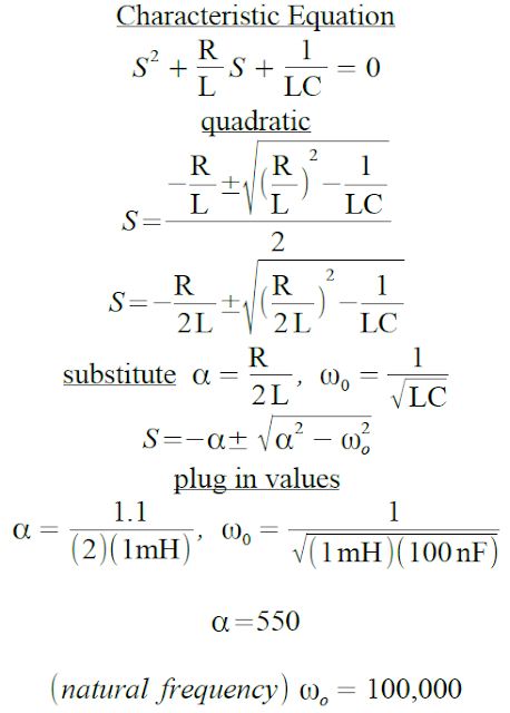
b) Natural frequency
Damping Ratio
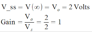
DC gain
 |
at T = INFINITY (STEADY STATE) |
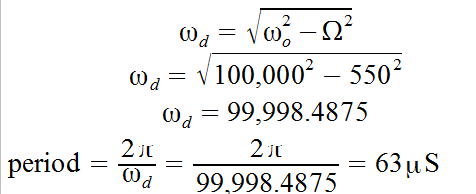
Period of oscillation
LAB
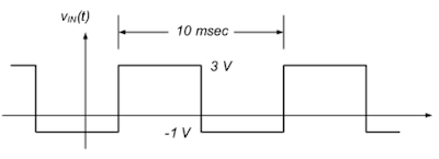
Construct circuit using 2 volt step input and a low frequency so that the circuit can reach a steady state before each pulse.
Results
We can see from the V(out) Oscilloscope on the top right of the figure below that the RLC circuit is UNDERDAMPED as predicted in the prelab. The oscilloscope on the left is V(in) of the 2v square wave, and the right shows the oscillations of V(out).
 |
| Underdamped 2nd order RLC circuit using TINKERCAD |
 |
| Underdamped RLC series circuit using EveryCircuit |
ANIMATION of Underdamped RLC circuit using EVERYCIRCUIT.
PART 2 CRITICALLY Damped Series RLC Circuit:
Prelab
Redesign circuit so its critically damped without affecting natural frequency.
Changing the resistor from 1.1 to 200 should make circuit critically damped.
LAB
Modify Circuit from Part 1 to create critically damped circuit without affecting natural frequency.
Results
RLC circuit is critically damped with resistor changed to 200 ohm's. Since L, and C are unchanged, natural frequency remains the same as in part 1.
The image below shows the circuit on a breadboard similar to Part 1, where the only change is the resistor from 1.1 to 200 ohms which gives a reading of critically damped as expected from prelab of Part 2 where there is no oscillations in V(out).
The image below shows the circuit on a breadboard similar to Part 1, where the only change is the resistor from 1.1 to 200 ohms which gives a reading of critically damped as expected from prelab of Part 2 where there is no oscillations in V(out).
|
|
| Critically Damped RLC circuit using TinkerCad App
We can see with the figure below, that V(in) is represented in orange and V(out) is represented in green, which shows no oscillations which is critically damped compared to Part 1 that was underdamped with oscillations.
|
 |
| Critically damped RLC series circuit using EveryCircuit. |
Animation of Critically Damped RLC circuit on EveryCircuit
Tuesday, October 17, 2017
10/17/17 Active RC Circuit Step Response
Active RC Circuit Step Response
Date: 10/17/17
Overview
Gain an understanding of passive versus active first order circuits. Passive circuits are useful in signal conditioning but arn't good at receiving additional loads which would require redesign of the circuit anytime a different load is applied to the circuit.
Active circuits are somewhat immune to different loads because the power supply comes from external sources.
Lab Procedures
1) Construct circuit from circuit diagram above, using resistors of 470 and a capacitor at 1µF.
2) Using a function generator, apply 4 volt peak-to-peak square water input with perioes = 10 ms (frequency = 100Hz)
3) Increase frequency to 300Hz, 500Hz, 1,000Hz, and 2,000Hz and comment on behavior.
Results
(100Hz)
 | |||||||||||||
| Active RC circuit using op-Amp741 with square wave Voltage input of 100Hz.
The figure below illustrates the capacitor voltage charge vs discharge at 100Hz, resulting in a saw tooth like wave.
adf
(300Hz)
(1,000Hz)
|
Tuesday, October 10, 2017
10/10/17 Non - Inverting Amplifier
Non - Inverting Amplifier
Date: 10/10/17
Overview
Gain an understanding of simple single operational amplifier-based circuit that are commonly used in circuits used to implement mathematical operations such as voltage gain within a circuit.
In this lab, we will gain an understanding of a non-inverting op-Amp (op-Amp27) circuit diagram and how to complete the circuit using a 8-pin op-Amp and see the relationship between Voltage(in) and Voltage(out).
Pre-Lab
a) Find gain ( Vout / Vin ) in the circuit.

b) Why is the circuit called a non-inverting voltage amplifier?
A inverting op-Amp provides an inverted polarity gain from voltage input in respects to voltage output, where as a non-inverting op-Amp provides a positive voltage gain.
d) For Voltage input, go from –3 volts to +3 volts in increments of .5 volts. Record results.
e) find slope

 |
| (independent power sources) |
 |
| (using Analog Discovery) |
A inverting op-Amp provides an inverted polarity gain from voltage input in respects to voltage output, where as a non-inverting op-Amp provides a positive voltage gain.
Lab Procedure
c) Apply +5 volts to Vcc(+) and -5 volts to Vcc(-)d) For Voltage input, go from –3 volts to +3 volts in increments of .5 volts. Record results.
e) find slope
Results (using both analog discovery and independent power sources)
 |
| Non-inverting op-Amp27 using Analog Discovery |
 |
| Non-Inverting opAmp27 using independent power sources |
Data collected for V(in) and V(out)
(analog discovery)
 |
| (data for analog discovery circuit) |
(independent power sources)
 |
| (independent power sources) |
 |
| (independent power sources) |
Plot of data
(analog discovery)
 |
| (non inverting op-Amp27 using Analog Discovery) |
 |
| (non inverting op-Amp27 using Analog Discovery) Slope (gain) = 2.5, which equals the same gain from prelab for analog discovery |
(independent power sources)
 |
| (independent power sources) |
Thursday, October 5, 2017
10/5/17Summing Amplifier
Summing Amplifier
Date : 10/5/2017
Overview
Summing two voltage inputs into a op-Amp commonly used in circuits to implement mathematical operations.The output voltage is an inverted and scaled version of the sum of the input voltages Va, and Vb. If R1 = R2, the input voltages are not individually scaled and the output voltage.
Note: R3 = R1, the output voltage is simply the sum of the two input voltages.
 |
| given circuit diagram of summing op-Amp |
Pre-lab
Design an inverting summing circuit which performs an addition of two voltage inputs. Note, circuit has a virtual ground.Lab Procedure
For 5 volts for Vcc(+) and Vcc(-)Set Vb to 1 volt.
Set Va to -4,-2,-1,0,1,2,3, and 5 volts. Record results
Results
 |
| Summing op-Amp741 circuit |
Data
 |
| Graph of Voltage (out) versus Voltage (a + b) |
Comments
Our results for our summing op-Amp regarding the calculated and actual were identical when using the op-Amp 741. I went ahead and when beyond the voltage input for Va to get values of positive and negative saturation. As seen, when values are within non saturation, and when R3 = R1, the output voltage is simply the sum of the two input voltages.
Below is verification the circuit using both TinkerCad and EveryCircuit to get a visual representation of the summing op-Amp.
 | |
|
 | |
|
Subscribe to:
Comments (Atom)


